Equipments
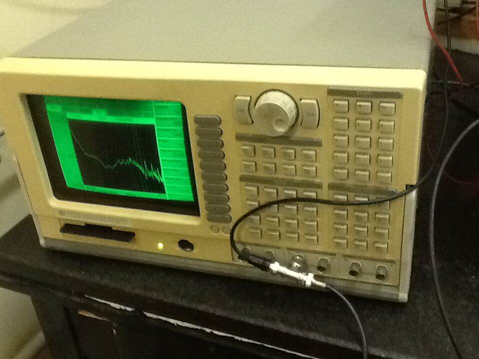
FFT spectrum analyzer
The laboratory has a Stanford Researchs spectrum analyzer model SR780. It uses the Fourier transform to generate a spectrum of intensity of each frequency contained in an electrical signal. It allows measurements of FFT, correlation, temporal histogram, cross-correlation among others. It has a bandwidth up to 102.4 kHz and enables the analysis of two-channel real time spectrum of an electrical signal.
Cryostats
The laboratory is equipped with two types of cryostat: a minor, which can be cooled to liquid nitrogen (N2) temperature of 77 K, and another with liquid helium (He), reaching temperatures between 10 and 300 K. Both cryostats are equipped with high quality connectors for electrical measurements, and quartz, zinc selenide or germanium windows for optical measurements.
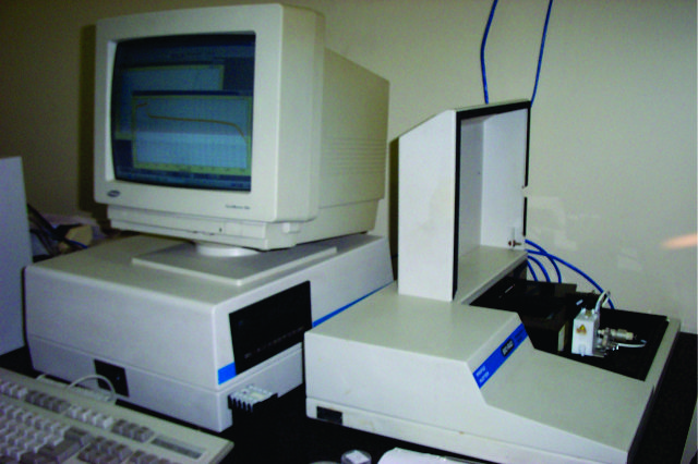
Current – voltage curves from cryogenic till room temperature
The IV curves measurement is the first step in the electrical characterization of devices. It provides the small current that flows into a device according to the applied voltage. In our laboratory, we use a semiconductor parameter analyzer HP 4145B. This equipment is responsible for applying the operating voltage (voltage bias) in the ± 20 Vdc ranges and ± 2 Vdc, and carries out the measurement of current in resolutions up to 1 picoampere (1x10-12 A).
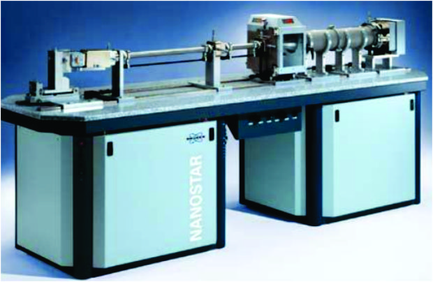
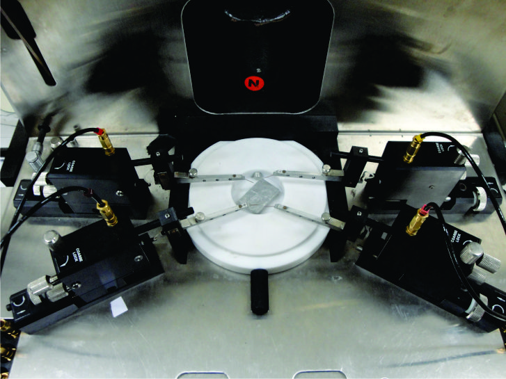
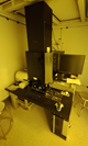
Difratômetro de baixo ângulo Nanostar
Copper tube, Vantec detector.
X-ray diffractometers
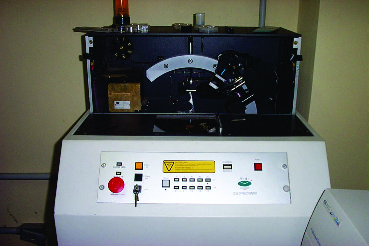
XRay diffraction equipment from Bede Scientific, model QC2a Diffractometer year 1989. It uses a x-ray source of 1,54054 ? (Cu K?1) wavelength and a GaAs 004 monochromator. This equipment is designed for Rocking Curve or Theta measurements and is optimized for thin films High Resolution aplications. It has a 1 arcsecond resolution and ranges till 10000 arcseconds.
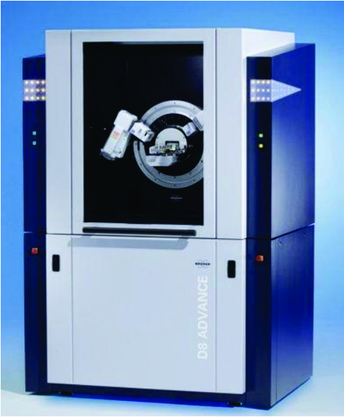
D8 Advance DaVinci
Silver and copper tubes, motorized sample holder, oven from -180° till 1600°C, LynxEye 500 detector, capillar sample holder.
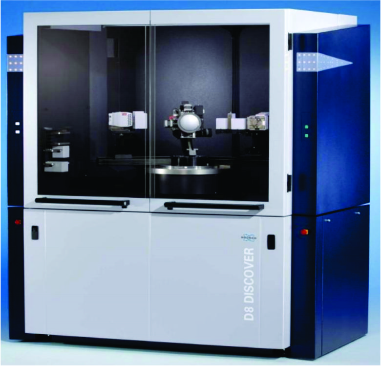
D8 Discover DaVinci
Copper tube, Göbel mirror, LynxEye detector, 4 mirrors monochromator, vertical Eulerian sample holder with 5 motorized movements, Bruker
Hall effect at 300 and 77 K
Model: HL5500 (Bio-Rad Microscience division). Magnet: 0.32 Tesla. Maximum resistivity measured in the order of M /cm² and minimum Hall voltage measured in the order of µV.
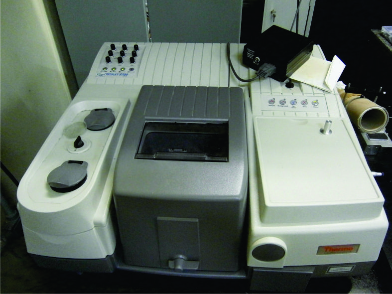
Fourier transform infrared spectrometer (FTIR) Nicole
The FTIR (Fourier transform infrared spectroscopy) technique is used when it is necessary to measure the infrared spectrum of a sample with respect to its absorption, emission or photocurrent. The Labdis has an Nexus 870 FTIR equipment with spectral range of 400 and 12000 cm-1 and resolution of 0.125cm-1.
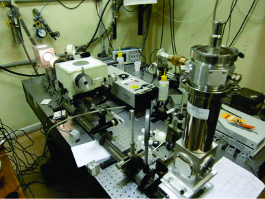
Spectroscopy: absorption, photoluminescence and photocurrent from cryogenic till room temperature
The spectroscopic measurements of photoluminescence and photocurrent can be performed for temperatures ranging 15 and 373K, with spectral range of 500 to 2500nm and resolutions up to 0.5nm.
For the photoluminescence the light source is an Ar+ laser with wavelength of 514nm.
The photocurrent can be performed with a white light source or with the FTIR unit, both with precision up to 1 pA.
The absorption measurement is performed inside the FTIR unit, so that its spectral range is between 400 and 12000 cm-1 with resolution of 0.125cm-1 .
Rapid Thermal Annealing
Oven used to perform thermal annealing of the samples for the formation of metal-semiconductor alloy required for making ohmic contacts. Capable of reaching temperatures up to 800°C. Annealing takes place in an atmosphere of N2 or Ar: H2 (forming gas).
Mask Aligner Karl Suss MA4
Developed for standard high-resolution photolithography, it uses an UV lamp with 10 mW/cm² intensity, enabling a micrometric resolution in ideal operating conditions. It supports up to four-inch wafers and fragments of any size. It is possible to use binary masks of up to five inches as well as transparencies and acetates.
Hotplate Prazitherm
The hotplate with precise temperature control is used to accomplish baking of the photoresist deposited on the surface of the sample. This baking is required to prepare the photoresist for the photolithographic process and etching.
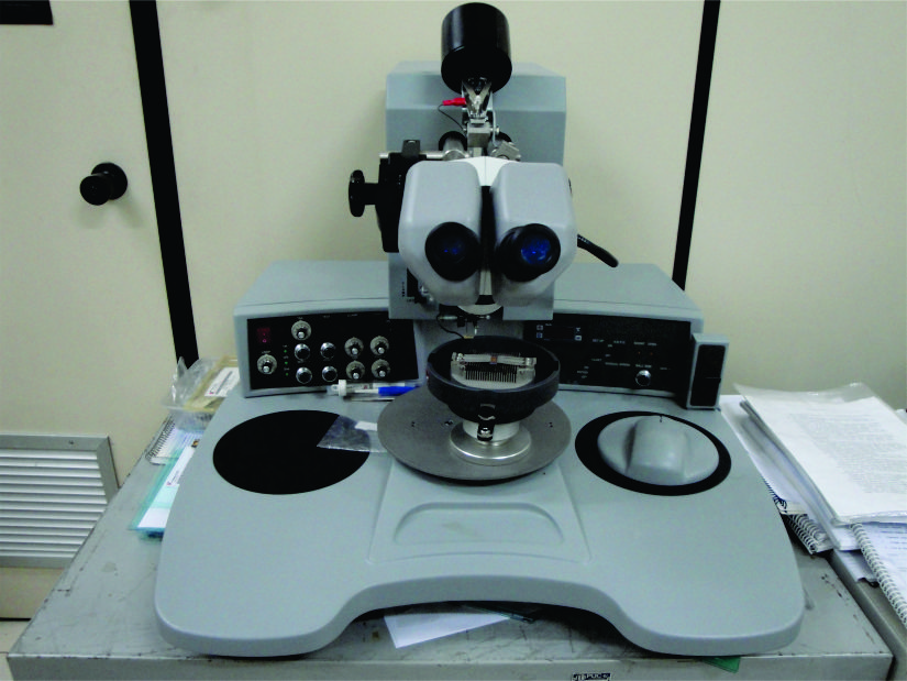
Atomic force microscope VEECO, model Nanoscope III
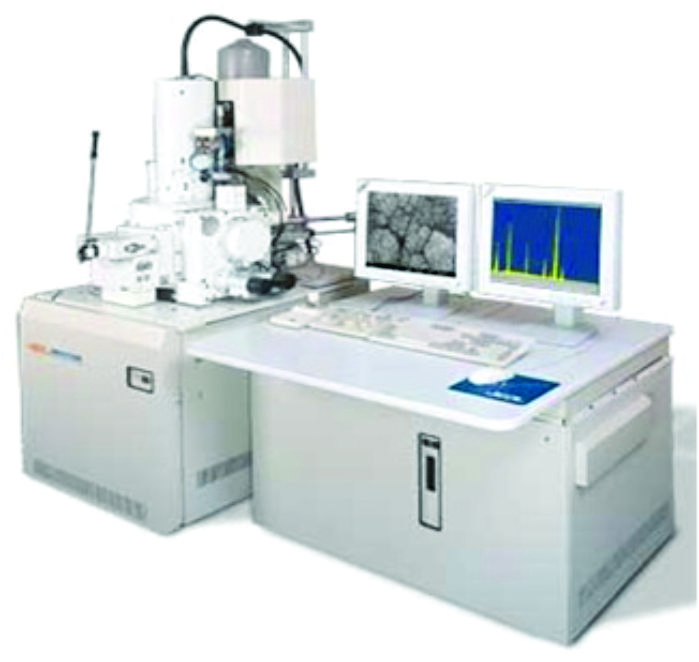
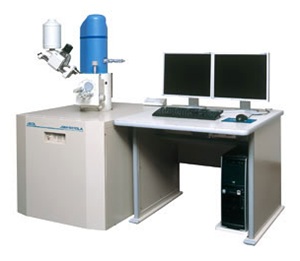
Scanning Electron Microscope
We have two scanning electron microscopes of JEOL enterprise. The scanning electron microscope JEOL JSM-6510/LV can operate in both high or low vacuum, and has a tungsten filament, being able to achieve maximum magnification of 300.000x and nominal resolution of 3nm. The second one is a field emission gun scanning electron microscope of high resolution JEOL JSM-6701F, achieving maximum magnification of 650.000x and 1nm of nominal resolution.
Both microscopes have a secondary electron detector able to give informations about the topography and of backscattered electron which gives a compositional information according to the atomic number of the elements. Both the microscopes work with the Thermo Scientific energy dispersive X ray spectrometer with a Noran software able to perform chemical analysis of points, area or complete regions of interest.
The JEOL JSM-6701F microscope also has a detector STEM dedicated to the scanning transmission mode. This kind of operation makes possible a morphological characterization and nanoanalysis of nanometric samples.
Wirebonder Kulicke & Soffa
It works in ballbonder and wedgebonder modalities. Used to prepare the electrical connections of the sample metal contacts between the sample holder and the chip-carriers, using Au wires with diameter of 25 microns.
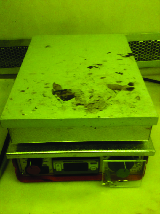
Capacitance – voltage profilometer at 300 K
The ECV (Eletrochemical Capacitance-Voltage) profiler is a capacitance-voltage measurement with electrochemical etching. Model: ECV Polaron PN4300 (Bio-rad Micro science division). The resolution limit in depth (interval between two measured points) depends on doping: for a doping of 1020cm-3 it is 1.3 nm, for 1019cm-3 it is 4 nm, for 1018cm-3 it is 13 nm, for 1017cm-3 it is 40 nm, for 1016cm-3 it is 130 nm, for 1015cm-3 it is 400 nm (not counting the inhomogeneity of the chemical etching). The range of carrier concentration that can be measured is between 1X10¹³ and 1X1020cm-3.

Profilometer for film and nanostructure thickness measurements
It allows the achievement of the surface relief profile of a sample. Used to measure micro roughness, corrosion depth and thickness of the deposited films. It uses a 12.5 microns radius tip, to achieve 5 angstrom vertical resolution, 400 angstroms horizontal resolution. The maximum measurement length is up to 162 mm.
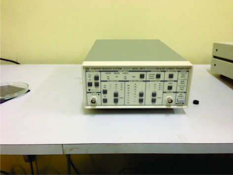
Current preamplifier
The SR570 Stanford Research current preamplifier employs a gain to amplify the devices output current signal and converts this current to a proportional voltage that can be measured. The gain ranges from 1 mA/V to 1 pA/V. The equipment also acts as a low noise voltage source, capable of applying voltages between -5 Vdc and 5 Vdc.
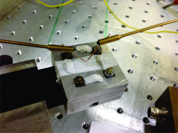
Probe station
The probe station allows the precise positioning of thin needles (controlled by micropositioners) on the surface of a semiconductor device. The contact of the probes with the device makes possible the electrical measurements of the semiconductor sample at room temperature without the need of performing electrical connections by wirebonder.
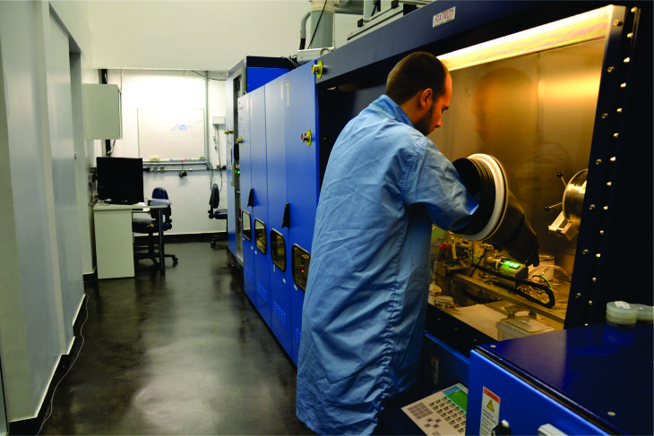
Cleanroom
The laboratory has a cleanroom facility where the entire sample processing is performed. It is an environment with controlled temperature and air humidity - about 22°C and humidity between 40 and 60% - and yellow lamps that allow the use of reagents sensitive to ultraviolet radiation.
The cleanroom also features a fume hood, as well as infrastructure for chemical etching needed to obtain patterns on the samples. Several organic solvents, acids, reagents, adhesives, developers and photoresists necessary for the processing of semiconductor devices are available.
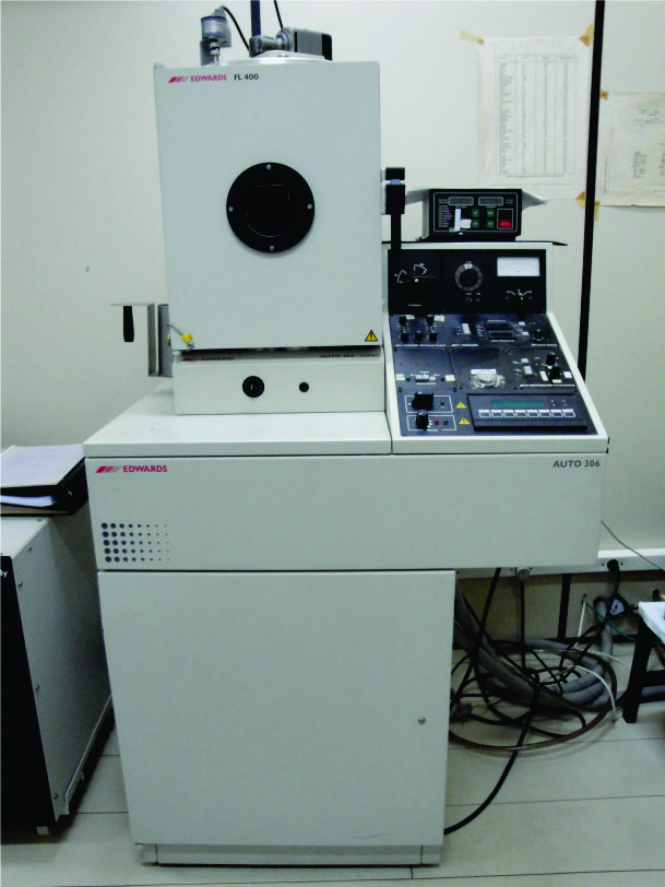
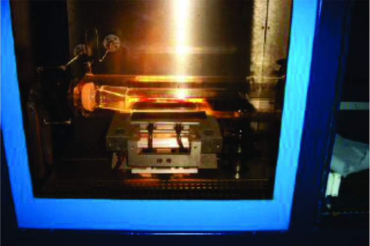
Thermal and ion beam evaporation equipment, Edwards
The Electron Beam Evaporation system is designed for controlled deposition thin metal films about tens angstroms thick. We have the following metals: Ni, Ge, Au, Ti, Zn, Cr and Pt.
System for growth of III-V semiconductors by metalorganic vapor phase epitaxy, Aixtron200 / 1989
Aixtron's equipment, model AIX200 year 1989, for epitaxial growth of III-V semiconductors using Al, In and Ga as group III materials, As and P as group V materials, Si as n dopant, and Zn or C as p dopants. It has the capacity to grow atomic monolayers of III-V semiconductors on GaAs or InP two inch substrate.
System for growth of III-V semiconductors by metalorganic vapor phase epitaxy, Aixtron200
Aixtron's equipment, model AIX200 year 2010, for epitaxial growth of III-V semiconductors using Al, In and Ga as group III materials, As and P as group V materials, Si as n dopant, and Zn and C as p dopants. It can grow atomic monolayers of III-V semiconductors on GaAs or InP two inch substrates. Also presents higher homogeneity due to substrate rotation during growth and higher control over the process due to an optical in situ measurement known as RAS (Reflectance Anisotropy Spectroscopy) through EpiRas equipment from Laytec.
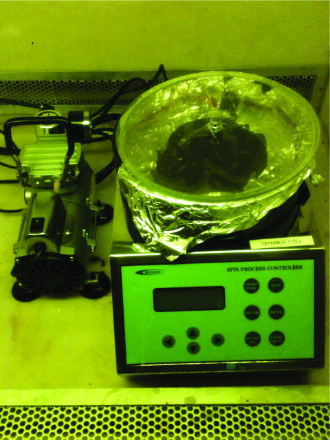
Spincoater Miolas
The spincoater is used for the deposition of photoresist films on surfaces of semiconductor substrates. The sample is fixed in a chuck capable of applying rotations of up to 10,000 rpm. This high rotation spreads the reactants on the sample surface, producing a film few microns thick that covers the entire surface.
Mask aligner OAI 300
Mask aligner for photolitography.
Equipment acquired with a grant from FAPERJ.